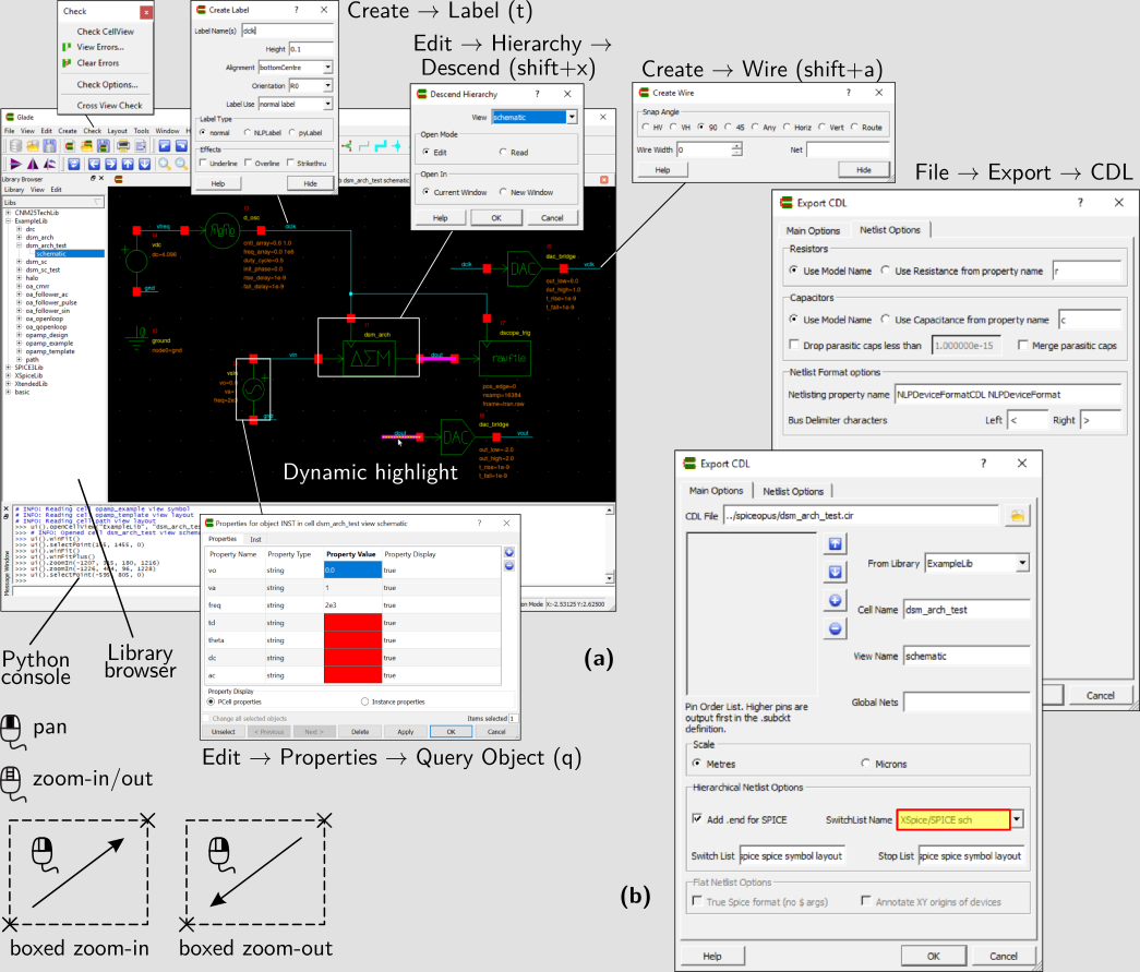
 Fig. 1
:
Glade schematic editor (a) and CDL export
dialogue configuration (b) for XSpice/SPICE
schematics. |
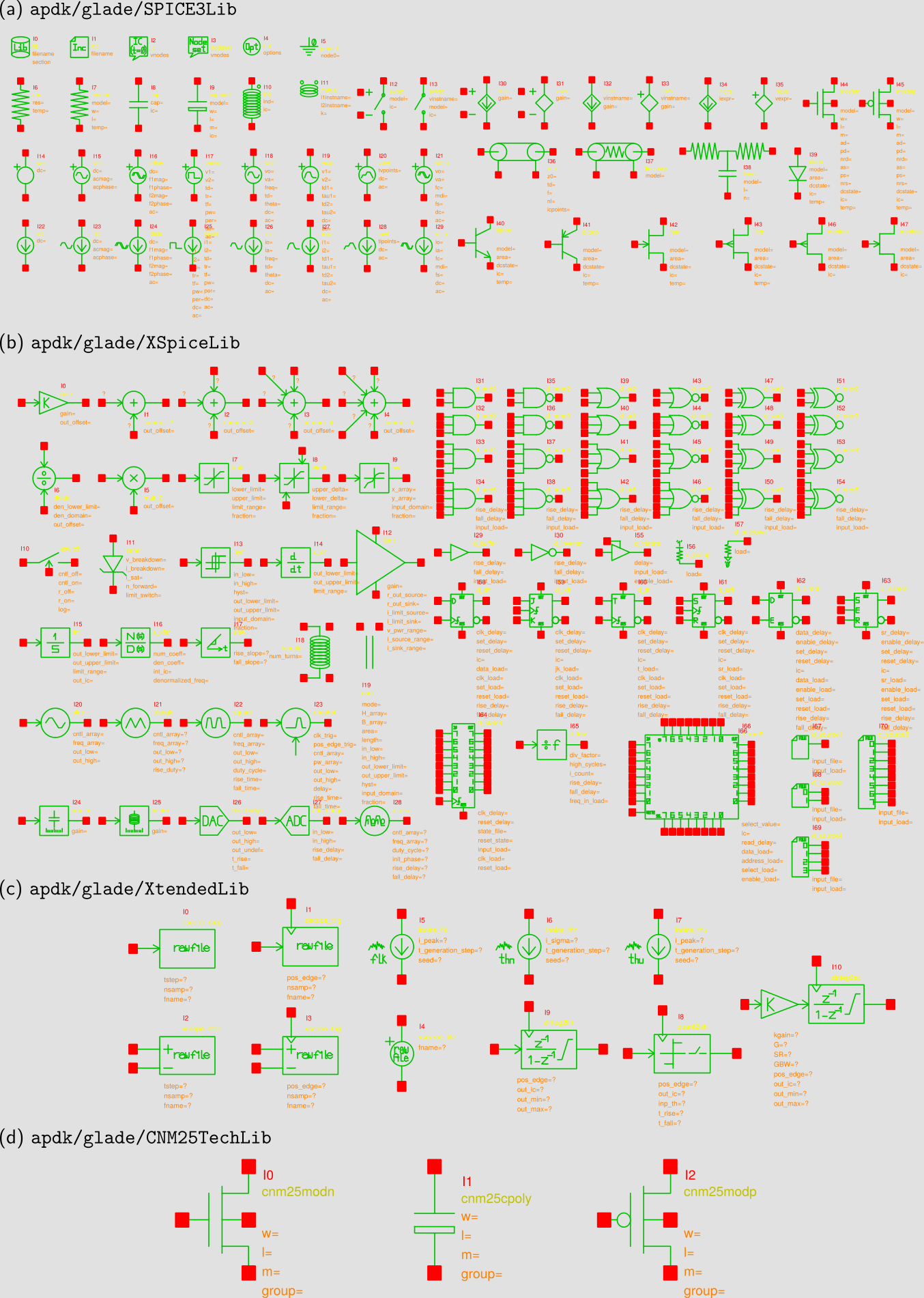
Fig. 2:
The full set of standard SPICE3 (a) and XSpice
(b), custom XSpice (c) and CNM25 (d) schematic
symbols available from the APDK reference
libraries.
|
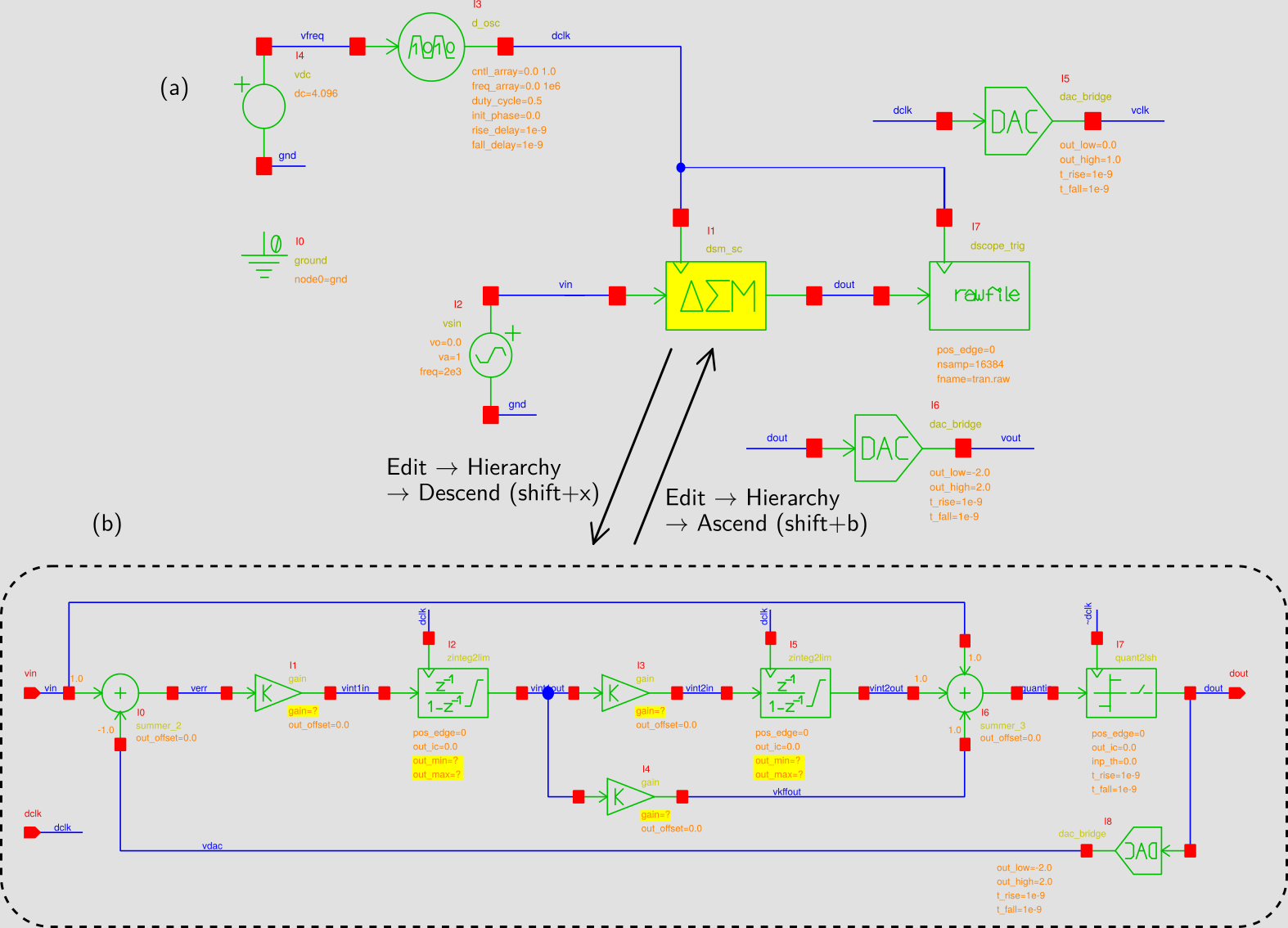
Fig. 3:
Test bench (a) and subcircuit (b) for the
differential-voltage DSM architecture. |

Fig. 4:
Main components of the SpiceOpus mixed-signal
simulation environment. Custom parts developed in
the frame of this APDK are highlighted in yellow. |
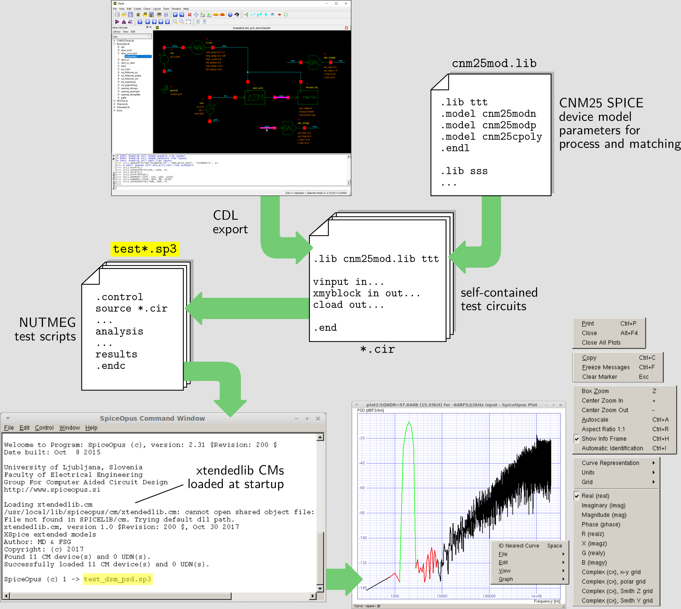
Fig. 5:
SpiceOpus simulation interface used in the APDK. |
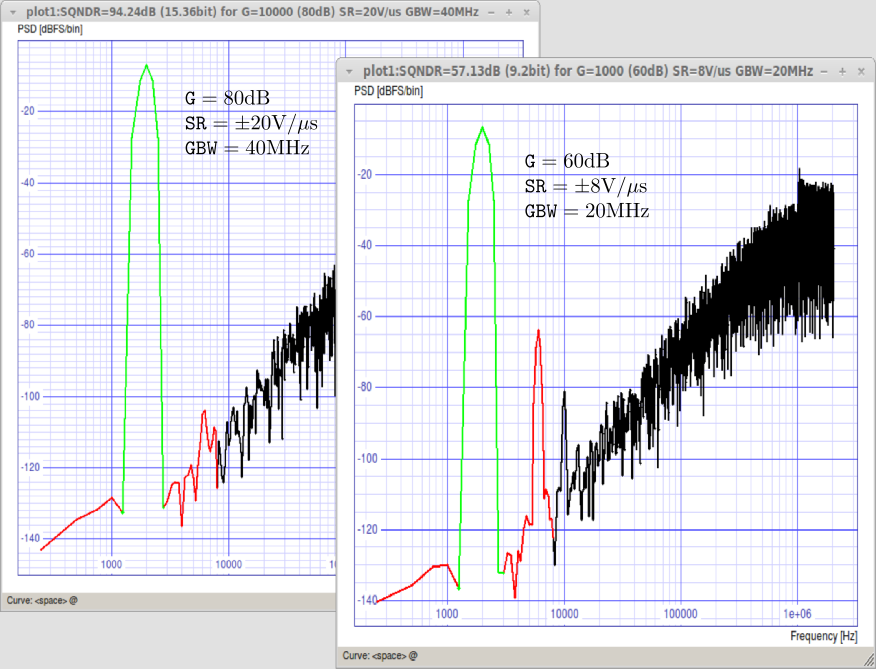
Fig. 6:
Example of XSpice results for the above DSM
architecture when changing the first integrator
OpAmp specs. |
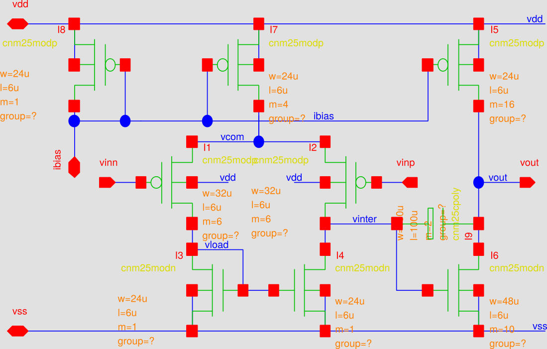
Fig. 7:
Glade schematic view of the CMOS OpAmp to be
optimized.
|
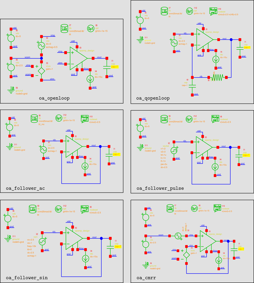
Fig. 8:
Test-bench schematics available for the
characterization of the OpAmp. |
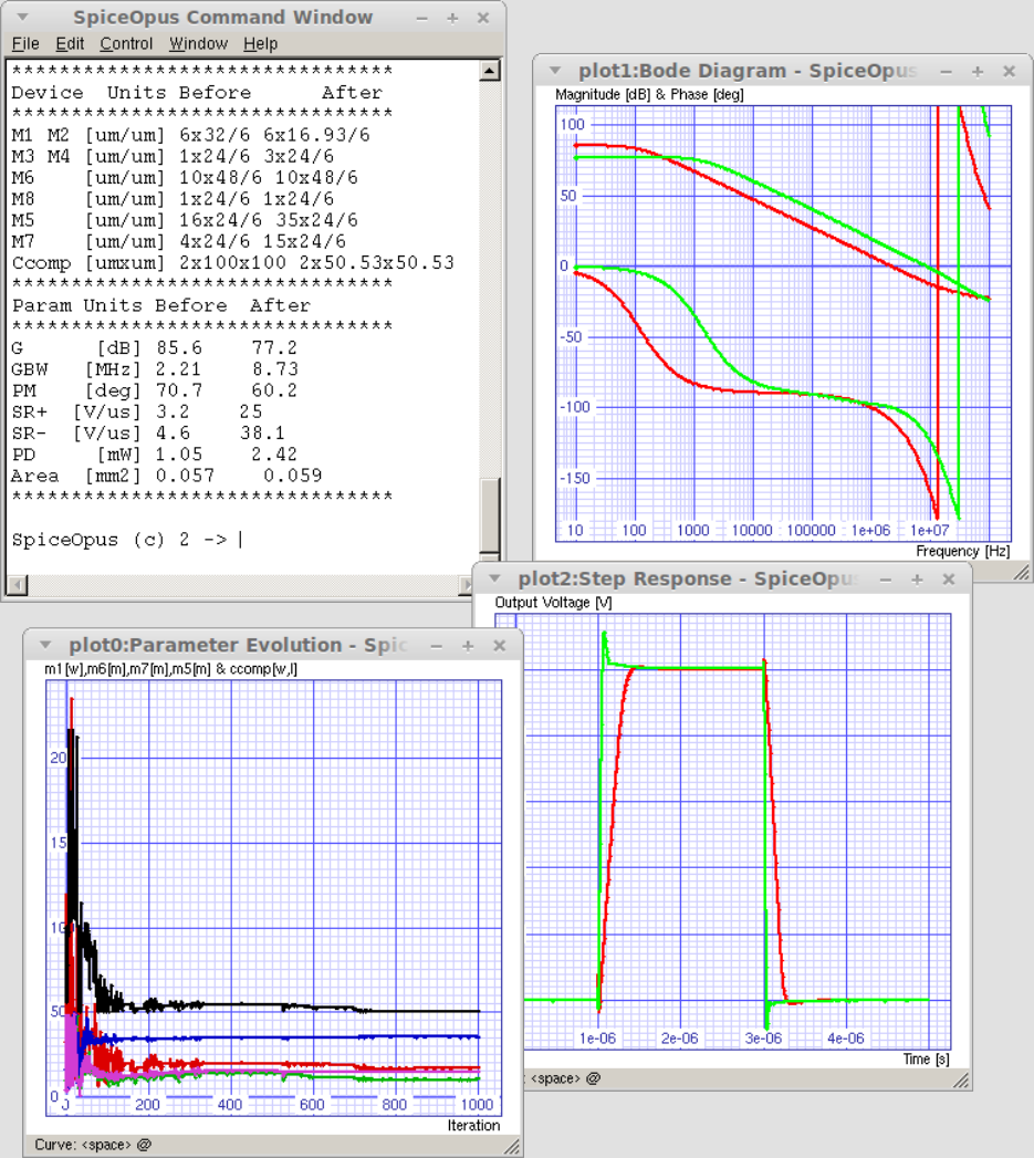
Fig. 9:
Example of SpiceOpus results obtained from the
optimize script of the OpAmp circuit. |
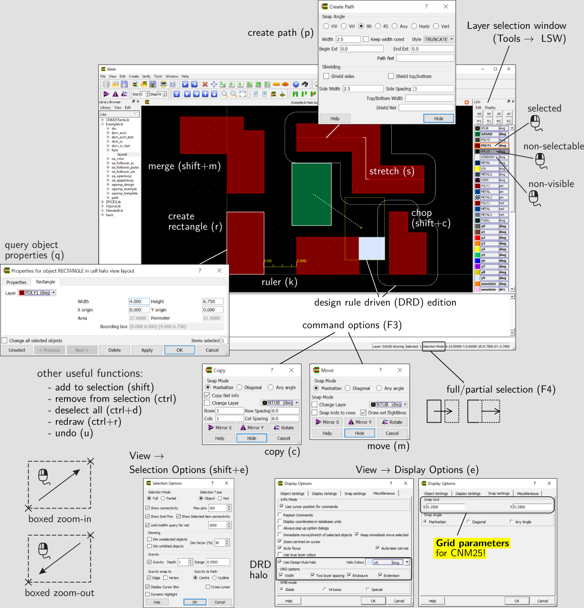
Fig. 10:
Glade layout editor and associated tools. |
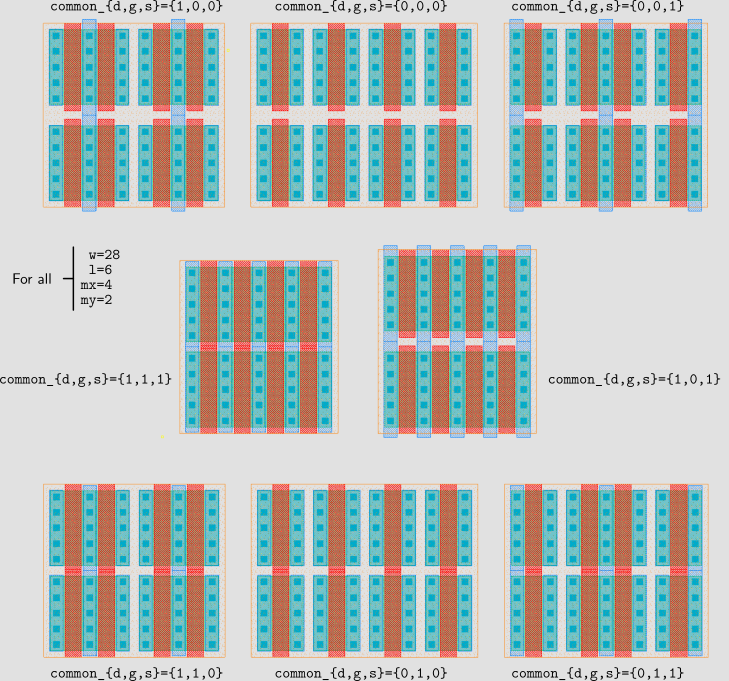
Fig. 11:
Example of Glade layout PCells available in the
CNM25 APDK.
|

Fig. 12:
Example of Glade create path command usage for
CNM25 routing.
|
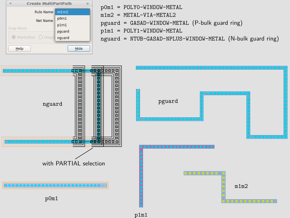
Fig. 13:
CNM25 automatic and stretchable structures
available through the Glade multi-part path (MPP)
command. |
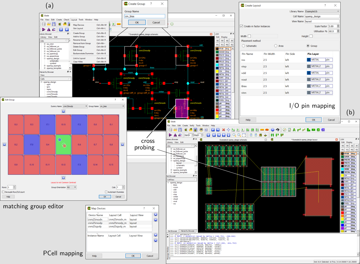
Fig. 14:
Usage of Glade layout generation tool for managing
matching groups (a) and for automated PCell
placement (b). |
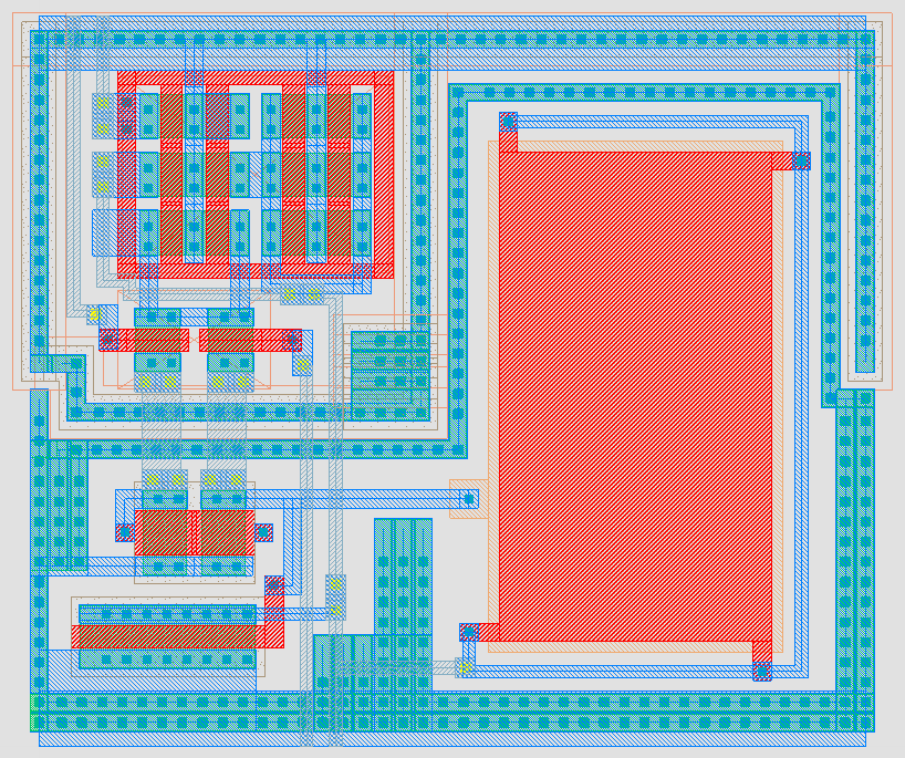
Fig. 15:
Example of OpAmp cell layout. |
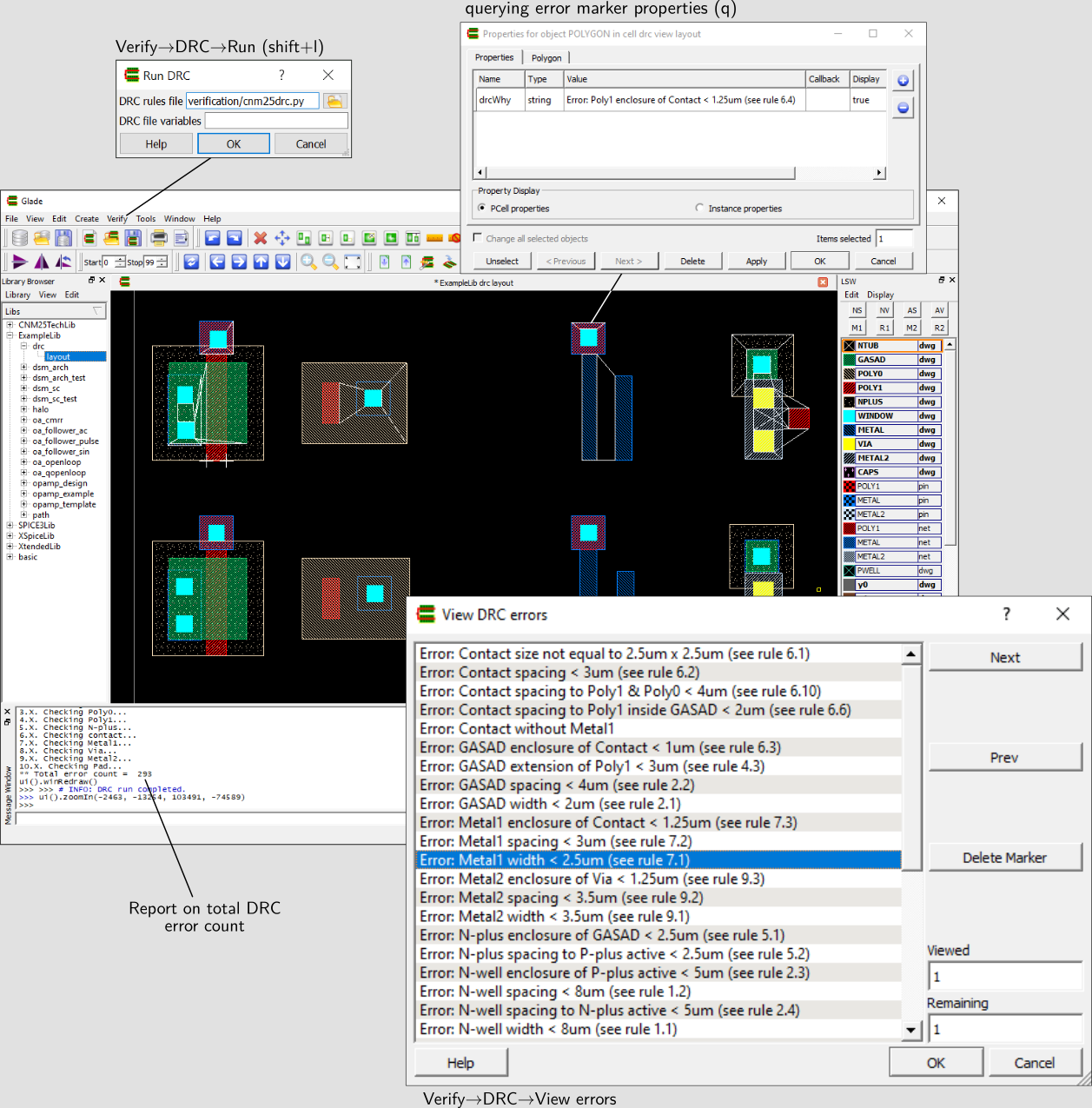
Fig. 16:
Example of Glade DRC error browsing. |
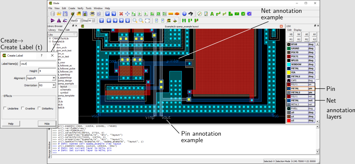
Fig. 17:
Glade layout view with pin and net annotation
examples. |
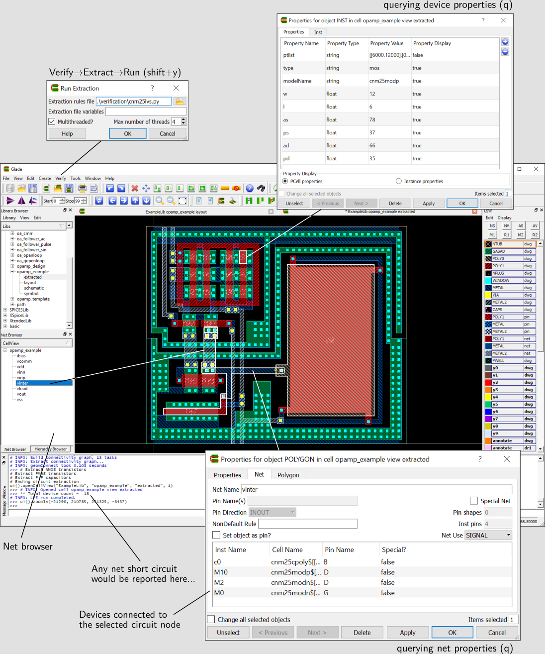
Fig. 18:
Glade extracted ERC inspection example. |
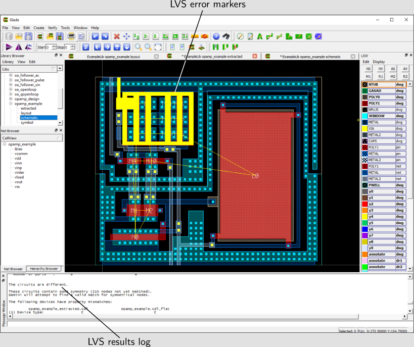
Fig. 19:
Example of Glade LVS error results.
|
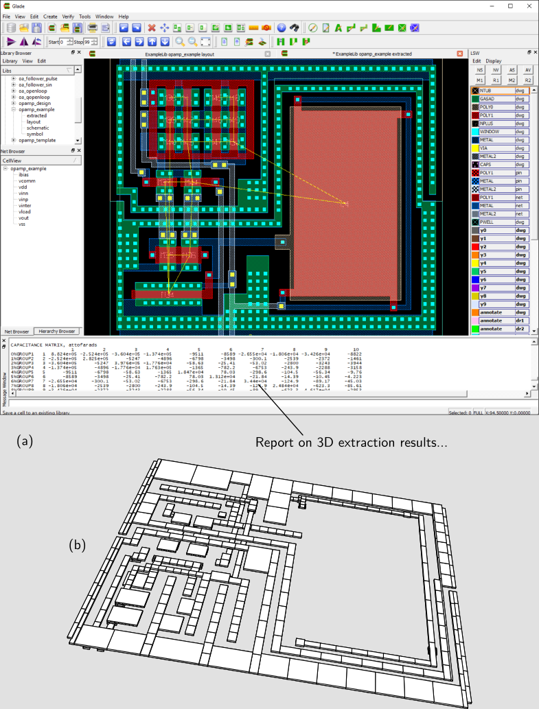
Fig. 20:
Example of Glade 3D extraction results (a) and
FastCap equivalent finite-element mesh (b). |